
[ad_1]
- SPHBM4 cuts pin counts dramatically whereas preserving hyperscale-class bandwidth efficiency
- Natural substrates scale back packaging prices and calm down routing constraints in HBM designs
- Serialization shifts complexity into signaling and base logic silicon layers
Excessive bandwidth reminiscence has advanced round extraordinarily large parallel interfaces, and that design alternative has outlined each efficiency and value constraints.
HBM3 makes use of 1024 pins, a determine that already pushes the bounds of dense silicon interposers and superior packaging.
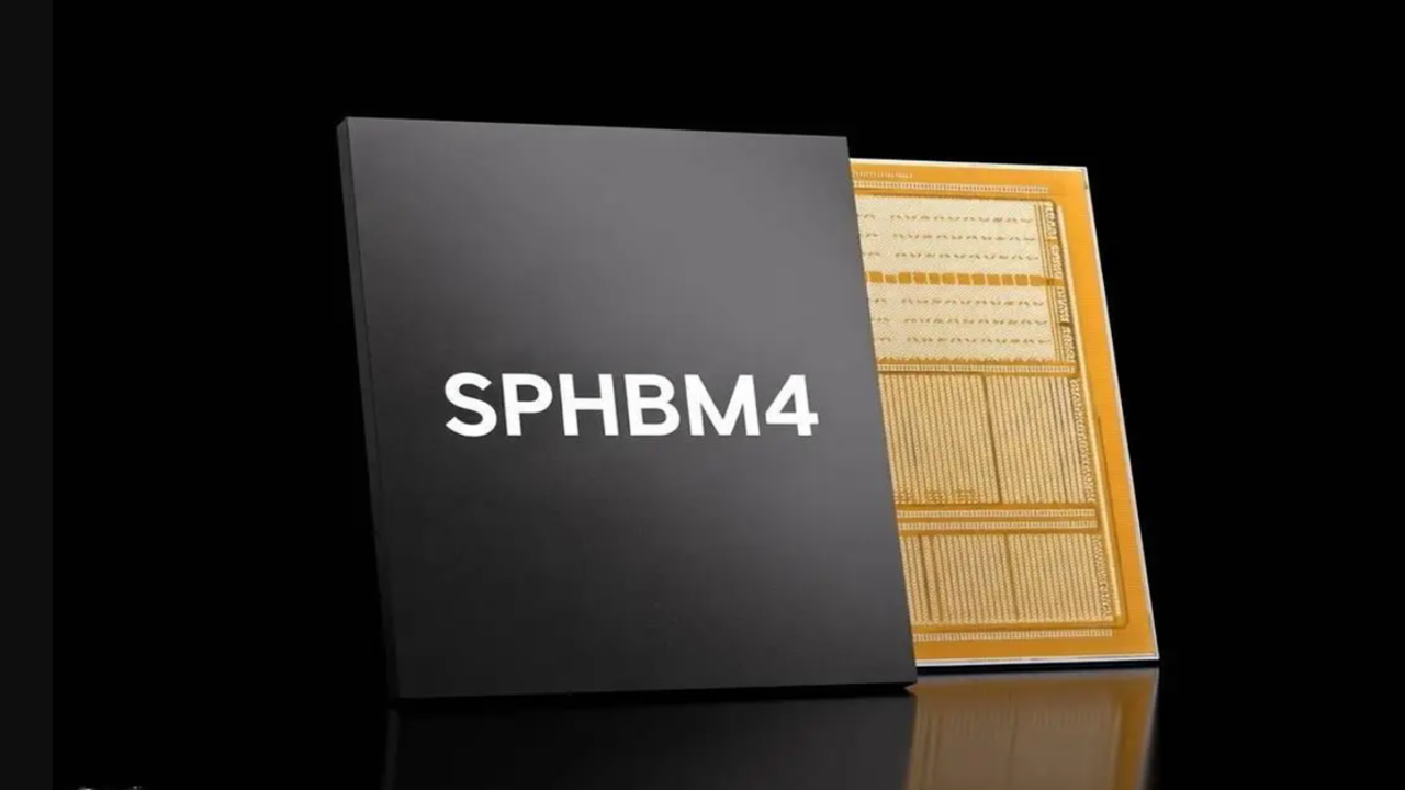
The JEDEC Stable State Expertise Affiliation is growing an alternate referred to as Commonplace Bundle Excessive Bandwidth Reminiscence 4 (SPHBM4), which reduces the bodily interface width whereas preserving whole throughput.
HBM4 interface doubles HBM3
The usual HBM4 specification doubles the HBM3 interface width to 2,048 pins, with digital alerts passing by way of every contact to lift mixture throughput.
This scaling method improves bandwidth, but it surely additionally will increase routing complexity, substrate calls for, and manufacturing expense, which considerations system designers.
The deliberate SPHBM4 system makes use of 512 pins and depends on 4:1 serialization whereas working at a better signaling frequency.
In bandwidth phrases, one SPHBM4 pin is predicted to hold the equal workload of 4 HBM4 pins.
This method shifts complexity away from pin rely and towards signaling know-how and base logic design.
Decreasing pin rely permits wider spacing between contacts, which straight impacts packaging choices.
JEDEC states that this relaxed bump pitch permits connection to natural substrates moderately than silicon interposers.
Silicon substrates assist very excessive interconnect densities with pitches above 10 micrometers, whereas natural substrates sometimes function nearer to twenty micrometers and value much less to fabricate.
The interposer connecting the reminiscence stack, its base logic die, and an accelerator would due to this fact transfer from a silicon-based design to an natural substrate design.
HBM4 and SPHBM4 gadgets are anticipated to supply the identical per-stack reminiscence capability, at the very least on the specification stage.
Nonetheless, natural substrate mounting permits longer channel lengths between the accelerator and reminiscence stacks.
This configuration could allow extra SPHBM4 stacks per bundle, which might improve whole reminiscence capability in contrast with typical HBM4 layouts.
Attaining this end result requires a redesigned base logic die, since SPHBM4 reminiscence stacks contain a four-to-one pin rely discount relative to HBM4.
HBM just isn’t general-purpose reminiscence and isn’t supposed for client methods.
Its use circumstances stay concentrated in AI accelerators, high-performance computing, and GPUs in information facilities operated by hyperscalers.
These consumers work at scales the place reminiscence bandwidth straight impacts income effectivity, which justifies continued funding in costly reminiscence applied sciences.
SPHBM4 doesn’t alter this utilization mannequin, because it preserves HBM-class bandwidth and capability whereas optimizing system-level price buildings that matter primarily to hyperscale deployments.
Regardless of references to decrease price, SPHBM4 doesn’t point out a path into client RAM markets.
Even with natural substrates, SPHBM4 stays stacked reminiscence with a specialised base logic die and tight coupling to accelerators.
These traits don’t align with DIMM-based client reminiscence architectures, pricing expectations, or motherboard designs.
Any price discount applies throughout the HBM ecosystem itself moderately than throughout the broader reminiscence market.
Nonetheless, for SPHBM4 to turn into a viable customary, it requires assist from main suppliers.
“JEDEC members are actively shaping the requirements that can outline next-generation modules to be used in AI information facilities…” mentioned Mian Quddus, chairman of the JEDEC Board of Administrators.
Main suppliers, together with Micron, Samsung, and SK Hynix, are JEDEC members and are already growing HBM4E applied sciences.
“Our #NuLink D2D/D2M #interconnect resolution has demonstrated the flexibility to attain 4TB/s of bandwidth in customary packaging, which is as much as 2x the bandwidth required by…HBM4 customary, so we look ahead to leveraging the work JEDEC has carried out with SPHBM4…” mentioned Eliyan, a base logic die semiconductor firm.
Through Blocks & Recordsdata
Comply with TechRadar on Google Information and add us as a most popular supply to get our skilled information, critiques, and opinion in your feeds. Be sure to click on the Comply with button!
And naturally it’s also possible to observe TechRadar on TikTok for information, critiques, unboxings in video type, and get common updates from us on WhatsApp too.
[ad_2]