Close Menu
VernoNews
  • Home
  • World
  • National
  • Science
  • Business
  • Health
  • Education
  • Lifestyle
  • Entertainment
  • Sports
  • Technology
  • Gossip
Trending

Lisa Vanderpump, Andy Cohen Say Upcoming ‘Vanderpump Guidelines’ Reunion is ‘Attractive’

January 18, 2026

ICE ‘wrongfully detained’ L.A. County D.A.’s workplace worker, Hochman says

January 18, 2026

This Week In Area podcast: Episode 193 — A Historical past of Tomorrow

January 18, 2026

Packers Head Coach Matt LaFleur Agrees to Multiyear Contract Extension

January 18, 2026

DeepSeek’s new Engram approach may slash AI reminiscence prices whereas boosting reasoning energy and easing international DRAM stress

January 18, 2026

Dueling protests in Minneapolis over ICE’s presence in metropolis

January 18, 2026

Trump can have the medal, however that doesn’t make him a Nobel Prize winner

January 18, 2026
Facebook X (Twitter) Instagram
VernoNews
  • Home
  • World
  • National
  • Science
  • Business
  • Health
  • Education
  • Lifestyle
  • Entertainment
  • Sports
  • Technology
  • Gossip
VernoNews
Home»Technology»This ultrafast laser trick modifications how chips deal with warmth lengthy earlier than followers and liquid cooling even matter
Technology

This ultrafast laser trick modifications how chips deal with warmth lengthy earlier than followers and liquid cooling even matter

VernoNewsBy VernoNewsJanuary 17, 2026No Comments3 Mins Read
Facebook Twitter Pinterest LinkedIn Tumblr Reddit WhatsApp Email
This ultrafast laser trick modifications how chips deal with warmth lengthy earlier than followers and liquid cooling even matter
Share
Facebook Twitter LinkedIn Pinterest WhatsApp Email


  • Warmth circulate is altered inside chip parts as an alternative of eliminated after buildup
  • Phonon movement is proscribed via nanoscale floor patterning
  • Ultrafast lasers allow nanoscale patterning at industrially related speeds

At present, most electronics depend on warmth sinks, followers, or liquid cooling as a result of the parts inside chips conduct warmth in mounted methods.

A brand new technique designed by Japanese researchers lets engineers management how briskly warmth escapes from a fabric, relatively than simply attempting to take away warmth after it builds up.

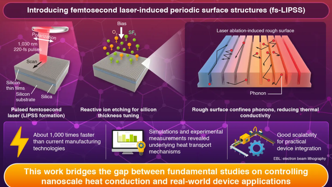
The work describes a laser-based fabrication technique that modifies how warmth strikes via skinny silicon and silica movies by instantly shaping their surfaces on the nanoscale.


You could like

Altering warmth transport on the chip part degree

The method depends on ultrafast laser pulses, every lasting a femtosecond, to ablate materials and create parallel grooves throughout the movie floor.

These grooves kind with rigorously managed spacing and depth that intently match the common distance phonons journey earlier than scattering.

As a result of phonons are the first carriers of warmth in these parts, proscribing their motion predictably alters general thermal conductivity.

The ensuing options, often known as femtosecond laser-induced periodic floor constructions, present excessive uniformity over comparatively massive areas.

Signal as much as the TechRadar Professional e-newsletter to get all the highest information, opinion, options and steerage your small business must succeed!

When mixed with typical dry etching to regulate movie thickness, the patterned surfaces exhibit a marked discount in thermal conductivity.

Thermoreflectance measurements quantified this modification, providing experimental affirmation relatively than inferred conduct.

Numerical simulations additionally confirmed that the discount arises primarily from restricted phonon journey distances relatively than modifications in chemical composition or bulk materials properties.


You could like

A central declare of the research issues fabrication velocity. The fs-LIPSS course of is reported to function at a throughput greater than 1000x quicker than single-beam electron-beam lithography whereas nonetheless reaching nanoscale decision.

This distinction is substantial, particularly for purposes requiring massive patterned areas, resembling thermal layers built-in into knowledge center-class processors.

The method is maskless and resist-free, which reduces procedural complexity and aligns with normal CMOS manufacturing constraints.

The method has additionally been described as able to wafer-scale implementation with out introducing further parts or lithographic steps.

As a result of the strategy avoids resists and masks, it stays appropriate with established semiconductor workflows.

The researchers describe the method as scalable, semiconductor-ready, and appropriate for integration with present fabrication strains.

The nanostructures are described as mechanically sturdy, with studies indicating energy ranges as much as 1000x greater than these produced utilizing some typical patterning approaches.

Nonetheless, the out there description offers restricted element on direct mechanical benchmarking or comparative testing strategies.

The method seems promising, and it’s related for high-performance computing, quantum gadgets, and thermal administration challenges related to dense GPU clusters powering fashionable AI instruments.

However wider adoption will rely upon reproducibility, long-term stability, and value below industrial situations, particularly at knowledge middle deployment scales.

Through Institute of Science Tokyo


Observe TechRadar on Google Information and add us as a most well-liked supply to get our skilled information, critiques, and opinion in your feeds. Be sure to click on the Observe button!

And naturally you may as well comply with TechRadar on TikTok for information, critiques, unboxings in video kind, and get common updates from us on WhatsApp too.


Avatar photo
VernoNews

Related Posts

DeepSeek’s new Engram approach may slash AI reminiscence prices whereas boosting reasoning energy and easing international DRAM stress

January 18, 2026

Block advertisements in your gadgets for all times for underneath $40

January 17, 2026

Gear Information of the Week: Kia Reveals off the EV2, and Fujifilm Debuts New Instax Cameras

January 17, 2026

Comments are closed.

Don't Miss
Gossip

Lisa Vanderpump, Andy Cohen Say Upcoming ‘Vanderpump Guidelines’ Reunion is ‘Attractive’

By VernoNewsJanuary 18, 20260

Lisa Vanderpump & Andy Cohen ‘Vanderpump Guidelines’ Reunion’s So Attractive!!! Revealed January 17, 2026 4:28…

ICE ‘wrongfully detained’ L.A. County D.A.’s workplace worker, Hochman says

January 18, 2026

This Week In Area podcast: Episode 193 — A Historical past of Tomorrow

January 18, 2026

Packers Head Coach Matt LaFleur Agrees to Multiyear Contract Extension

January 18, 2026

DeepSeek’s new Engram approach may slash AI reminiscence prices whereas boosting reasoning energy and easing international DRAM stress

January 18, 2026

Dueling protests in Minneapolis over ICE’s presence in metropolis

January 18, 2026

Trump can have the medal, however that doesn’t make him a Nobel Prize winner

January 18, 2026
About Us
About Us

VernoNews delivers fast, fearless coverage of the stories that matter — from breaking news and politics to pop culture and tech. Stay informed, stay sharp, stay ahead with VernoNews.

Our Picks

Lisa Vanderpump, Andy Cohen Say Upcoming ‘Vanderpump Guidelines’ Reunion is ‘Attractive’

January 18, 2026

ICE ‘wrongfully detained’ L.A. County D.A.’s workplace worker, Hochman says

January 18, 2026

This Week In Area podcast: Episode 193 — A Historical past of Tomorrow

January 18, 2026
Trending

Packers Head Coach Matt LaFleur Agrees to Multiyear Contract Extension

January 18, 2026

DeepSeek’s new Engram approach may slash AI reminiscence prices whereas boosting reasoning energy and easing international DRAM stress

January 18, 2026

Dueling protests in Minneapolis over ICE’s presence in metropolis

January 18, 2026
  • Contact Us
  • Privacy Policy
  • Terms of Service
2025 Copyright © VernoNews. All rights reserved

Type above and press Enter to search. Press Esc to cancel.