
[ad_1]
- Photonic chips with quantum lasers are lastly being constructed with out redesigning the entire system
- These lasers work straight on silicon and nonetheless survive excessive warmth for over six years
- College of California researchers crammed the laser hole with polymers and nailed precision beam management on-chip
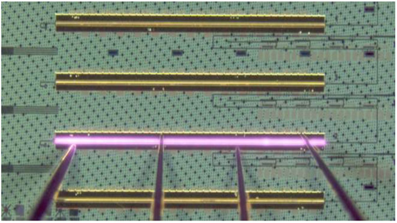
A brand new fabrication methodology may make photonic circuits cheaper and extra sensible by straight integrating quantum dot (QD) lasers onto silicon chips, a course of that might affect how future sensible residence gadgets, health trackers, and even laptops are engineered.
The analysis group, led by Rosalyn Koscica on the College of California, achieved this by combining three key methods.
They used a pocket laser configuration for direct integration, adopted a two-step progress methodology involving metalorganic chemical vapor deposition and molecular beam epitaxy, and launched a polymer gap-filling approach to cut back optical beam unfold.
Closing the hole with cautious engineering
This improvement addresses longstanding challenges involving materials incompatibilities and coupling inefficiencies which have traditionally restricted the efficiency and scalability of built-in photonic programs.
The mixed efforts minimized the preliminary interface hole and made it potential for lasers to perform reliably on silicon photonic chiplets.
Because the researchers notice, “Photonic built-in circuit (PIC) purposes name for on-chip mild sources with a small system footprint to allow denser element integration.”
The brand new strategy permits steady single-mode lasing on the O-band frequency, which is well-suited for knowledge communications in knowledge facilities and cloud storage programs.
By integrating the lasers straight with ring resonators fabricated from silicon or utilizing distributed Bragg reflectors from silicon nitride, the group has additionally addressed points associated to alignment and optical suggestions.
One of many extra shocking findings from the analysis is how properly the lasers carry out beneath warmth.
“Our built-in QD lasers demonstrated a excessive temperature lasing as much as 105 °C and a life span of 6.2 years whereas working at a temperature of 35 °C,” says Ms. Koscica.
These efficiency metrics recommend a stage of thermal stability beforehand tough to attain with monolithically built-in designs.
This thermal resilience opens the door to extra sturdy purposes in real-world environments, the place temperature fluctuations can restrict the reliability of photonic elements.
It could additionally scale back the necessity for lively cooling, which has historically added price and complexity to previous designs.
Past efficiency, the combination methodology seems properly suited to large-scale manufacturing.
As a result of the approach may be executed in commonplace semiconductor foundries and doesn’t require main adjustments to the underlying chip structure, it holds promise for broader adoption.
The researchers argue that the tactic is “cost-effective” and “can work for a spread of photonic built-in chip designs while not having in depth or complicated modifications.”
That stated, the strategy will doubtless face scrutiny concerning consistency throughout massive wafers and compatibility with industrial photonic programs.
Additionally, success in managed lab environments doesn’t assure seamless deployment in mass manufacturing settings.
Nonetheless, the mix of a compact laser design, compatibility with standard processes, and integration of O-band performance makes this improvement notable.
From knowledge facilities to superior sensors, this silicon-compatible laser integration may carry photonic circuits nearer to mass-market viability.
Through IEEE
You may also like
[ad_2]